 Automation Research & Embedded Technologies
Certificate Verification
Automation Research & Embedded Technologies
Certificate Verification
Automation Research & Embedded Technologies
Certificate Verification
Automation Research & Embedded Technologies
Certificate Verification
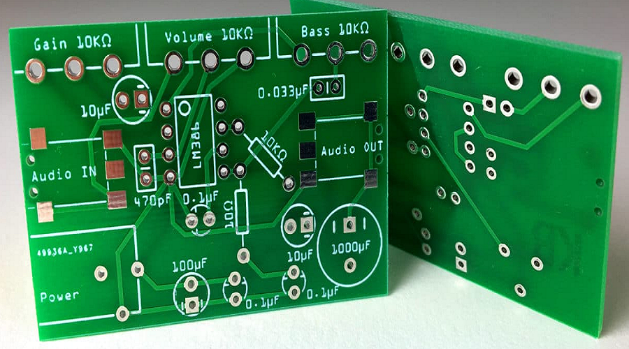
" Printed Circuit Board (PCB) ছাড়া ইলেকট্রনিক্স প্রোডাক্ট বানানো সম্ভব না। PCB হচ্ছে কম্পিউটার, ল্যাপটপ, সেলফোনসহ প্রায় সকল Electronic Gadget এর মূল উপাদান। ইলেকট্রনিক্স ইন্ডাস্ট্রি PCB ছাড়া কল্পনাই করা যায় না। আর এ কারণেই দিনদিন PCB ডিজাইনারদের ডিমান্ড বেড়েই চলছে। PCB Design শিখে স্কুল, কলেজ বা ভার্সিটির প্রজেক্ট কাজ ছাড়াও অনলাইন মার্কেটপ্লেসে ফ্রিল্যান্সিং করে ঘরে বসে প্রচুর টাকা ইনকাম করা সম্ভব। তাই ইলেকট্রনিক্স ইন্ডাস্ট্রিতে ক্যারিয়ার ডেভেলপ করতে চাইলে আজই এই কোর্সে এনরোল করুন।"
admission formCourse Title:
PCB design & Fabrication
Course Duration:
10 Days
Total No. of seats:
10 seats
Prerequisites:
Basic understanding of electrical systems, automation, and control systems.
Course Fee: BDT 4000.00
PCB design & Fabrication 10-Days Course Syllabus
Day 1: Introduction to PCB Design - Overview of Printed Circuit Boards (PCBs) - PCB types (Single-layer, Double-layer, Multilayer, Flexible) - Basics of Electrical and Electronic Circuits - Importance of PCB design in electronics manufacturing Day 2: PCB Design Tools - Introduction to PCB Design Software ( Proteus, Altium Designer) - Setting up a PCB project in the design software - Schematic capture and circuit design - Component selection and library management in design tools Day 3: Schematic Design - Drawing circuit schematics in PCB design software - Component placement and connections - Electrical rules check (ERC) - Best practices for schematic design Day 4: PCB Layout Design - PCB layout basics: component placement, routing, and trace design - Layer management (single, double, multilayer PCBs) - Design rules check (DRC) - Understanding PCB track widths, via sizing, and clearance Day 5: Power and Ground Planes - Importance of power and ground planes in PCB design - Creating planes and copper pours - Minimizing noise and EMI (Electromagnetic Interference) - Grounding techniques for signal integrity Day 6: Signal Integrity and PCB Design for High-Speed Circuits - Introduction to signal integrity issues (crosstalk, reflections) - Design techniques for high-speed PCBs (controlled impedance, differential pairs) - PCB trace routing strategies for signal integrity - Via placement and signal return paths Day 7: PCB Design for Manufacturability (DFM) - Understanding manufacturing constraints in PCB design - Design for manufacturability (DFM) guidelines - Thermal management in PCB design (heat dissipation, component placement) - Panelization and optimization for PCB production Day 8: PCB Fabrication Process - Overview of PCB fabrication steps - Materials used in PCB fabrication (FR4, copper, solder masks) - Drilling, etching, and layer alignment processes - Surface finishes (HASL, ENIG, OSP) Day 9: PCB Assembly and Testing - Introduction to PCB assembly processes (SMT, Through-hole) - Soldering techniques (hand soldering vs. reflow soldering) - Visual inspection and testing methods (AOI, X-ray inspection) - Electrical testing of PCBs (continuity, functional testing) Day 10: Hands-on PCB Design and Fabrication Project - Designing a simple PCB circuit from scratch - Generating Gerber files and Bill of Materials (BOM) - Submitting the design for fabrication - Assembling and testing the fabricated PCB * Certification of course completion.Get the certificate